We use cookies in order to optimize your user experience. Several cookies are necessary to
operate the site, while others are used for statistical purposes, to provide user-friendly
settings, or to display personalized content. You can decide for yourself which cookies you
wish to allow. Please note that some of the site’s functions may be unavailable as a result
of your settings. You can find further information in our data privacy statement.
Show details
Miniaturization
The trend towards miniaturization is not to stop and the market calls for ever smaller, lighter and more powerful products with higher functionality. Typical examples are hearing instruments that fit into the ear channel and mobile phones with integrated camera and GPS that double as PDAs and MP3 players with the capacity to store thousands of songs.
This trend leads to a demand for smaller, thinner and more highly integrated (HDI) PCBs that are populated with flip chip and micro BGA or on which bare dies are bonded (chip & wire technology). Further increase in form factor is achieved through 3D devices which require substrates that can be folded in appropriate areas.
Below are examples of technologies that allow to achieve a high degree of miniaturization.
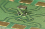
Flip Chip Technology
The flip chip technology is the most space economic assembly method. A bare die with special attachment pads and solder balls is flipped and soldered to a substrate. Other interconnect methods such as stud bumping with conductive adhesive are also utilized. As no wires are present, this technology has low connecting impedances and therefore favorable high frequency proprieties. This technology is used on flexible PCBs as well and is then known as chip on flex (COF).
On the PCB side the challenges are very small dimensions and high pitch of the openings in the solder mask as well as a high density of contact pads that need to be routed.
GS Swiss PCB AG has the capability to manufacture solder mask with very fine structures by either exposing the solder mask with laser or by ablating cured solder mask with a laser beam. For designs with a high pitch, copper filled micro vias in the pads (via in pad) can be used. The PVA-Technology which is a combination of copper filled vias with sequential build up (stacked vias) makes maximum packing density and integration possible.
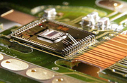
Wire Bonding
Wire bonding is a method of making interconnections between bare dies and a PCB by connecting the connecting pads of the chip and the landing pads on the substrate with very thin gold or aluminum wires. The wires are attached on both ends using some combination of heat, pressure and ultrasonic energy to produce a weld.
To achieve a high quality of the wire connections and high assembly yields, the thickness and composition of the nickel and gold as well as the condition of the gold surface are crucial. Any defect on the landing pad can either reduce the weld strength or cause the fragile bonding needle to break.
Owing to experience of many years GS Swiss PCB AG is knowledgeable about the requirements for gold surfaces and has a wide range of gold surfaces available (flash gold, reductive gold, Ni/Pd/Au as well as electroplated and hard gold). If required, PCBs can be plated with two different gold surfaces.
In order to achieve a constant quality of the surfaces the gold and nickel baths are examined periodically and the thickness of the nickel and gold plating measured by x-ray spectrometry and recorded. In final inspection specifically trained employees are inspecting the bond pads by microscope equipped with specific filters.